Miss Parker technical details
Homepage Miss Parker VirtuAL3101 Effect resources MFx News Links Contacts
General information Specification Technical details Miss Parker Plus Miss Parker Manager Download page
Schematic
Here are the schematics of Miss Parker v1.1: main board and user interface.
Here is the schematic of the Miss Parker Plus v1.0 extension. More details to be found on the Miss Parker Plus page.
All basic blocks defined in the specification page can be found back in the schematic: micro-controller, DSP, AD/DA, power supply...
Layout
Here is the placement, value/placement and BOM of the components of Miss Parker's main PCB and the Gerber files of the layout.
Here is the placement, value/placement and BOM of the components of Miss Parker's user interface PCB and the Gerber files of the layout.
Here is the value/placement and BOM of the components of Miss Parker Plus extension PCB.
The PCBs are dual layer ones and they have been manufactured by a specialized company, read the release note for more details about the files.
Note that the three boards have been validated now. The extension board is suffering some bugs though (lines inverted forbidding to use external mode of the AL3201) so if you want to build one, please contact Whity first.
Pictures
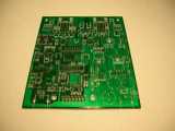
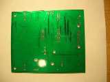
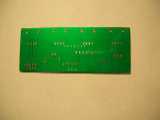
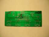
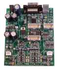
Here are pictures of the empty v1.1 PCB (main board and interface board):


Thanks a lot to Marek for the pictures and mainly for "daring" to launch production of a batch of these boards before doing the first beta test.
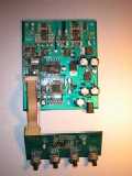
Here is a picture of the working v1.1 main board and v1.1 interface PCB:

The new main board improves the SNR from ~70dB to -90dB and corrects the bugs from the previous 1.0 version.
The new interface board will definitely improve the robustness of potentiometers against shocks, ...
Thanks again to Marek for these boards.
Here is a picture of the now old empty v1.0 PCB:

These are pictures of the populated v1.0 PCB:


Copyright © 2003 Axoris - Last modified: 2009-03-11


